OPERATIONAL AMPLIFIERS
The operational amplifier is a direct coupled , high gain, high input impedence , and low output impedence ,high bandwidth amplifier. The gain can be controlled by feedback by feedback . In short operational operational amplifiers are termed as "op-amp" ,op-amp are in performing various mathematical operation such as addition ,subtraction etc ,And it is mainly used in converting sine wave to square wave in future posts .
The block diagram of operational amplifier is shown below
if you want to understand the working of op-amp you need to understand working of differential amplifier . In my first post i briefly explained the working of differential amplifier . I think u read that
op-amp consists of 4 blocks
input stage :- Input consists of differential amplifier which gives high CMRR {The necessity of high CMRR is since it take 2 inputs, CMRR tells the ability to reject common signals [noise] & amplify differential signals} high input impedence , high voltage gain .
OPERATIONAL AMPLIFIERS
The operational amplifier is a direct coupled , high gain, high input impedence , and low output impedence ,high bandwidth amplifier. The gain can be controlled by feedback by feedback . In short operational operational amplifiers are termed as "op-amp" ,op-amp are in performing various mathematical operation such as addition ,subtraction etc ,And it is mainly used in converting sine wave to square wave in future posts .
The block diagram of operational amplifier is shown below
 |
| block diagram of operational amplifier |
op-amp consists of 4 blocks
input stage :- Input consists of differential amplifier which gives high CMRR {The necessity of high CMRR is since it take 2 inputs, CMRR tells the ability to reject common signals [noise] & amplify differential signals} high input impedence , high voltage gain .
Gain stage :- The gain of op-amp is further increased by gain stage, which consists of darlington pairs (CC-CC) AND (CC-CE) cascaded amplifier . here gain is the ratio of input by output and impedence resistance of ac circuit DC-LEVEL:-since op-amp is basically DC amplifier and no capacitor used , quiescent voltage shifts after every stage .To bring it back to the original level emitter follower is used as DC level shifter
Output stage :- output stage have low output impedence and should be able to supply high output current [ just remember the ohm's law as when resistance is low ,current will be higher ].it uses the pushpull amplifier to do like that .
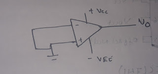
when the inputs of an op-amp are grounded the output must be zero . but there is a small error voltage at the output due to the difference in Vbe values of input transistors.
thanks for reading the article , in next article we study by using the different feedbacks what will be the output and characteristics
 |
| circuit diagram og op-amp |
A positive input at the inverting terminal produces inverted (negative) voltage at output. A positive input at non inverting terminal produces [positive] or non inverting voltage at output .
CHARACTERISTICS OF OP-AMP
- OPEN LOOP GAIN :- The gain of the amplifier without feed back is called the open loop gain.Here feedback means process of taking a part of output and feeding it back to the input is called feedback . The main thing here feedback is done through resistor . there are two types of feedback are there ,they are 1)positive feedback and 2) negative feedback
- INPUT IMPEDENCE :- impedence as seen from the input terminals
- OUTPUT IMPEDENCE:- impedence as seen from the output terminals (It tells us how many number of devices at the output without getting loaded).
- BAND WIDTH :- Ideal op-amp the bandwidth is infinite , which means that op-amp provides amplified output for signals of frequency from 0 to infinity hertz without any attenuation.
- CMRR :- Indicates the ability of op-amp to rejects the common mode signals (noise ) and amplify differential signals .
- SLEW RATE :- The maximum rate of change of output voltage per unit time . This character indicates the ability to respond to variation in the input frequency .
- INPUT OFFSET VOLTAGE :-
This is the small voltage that must be applied between the two input terminals to make output voltage zero . This is called balancing technique .
circuit diagram of input offset voltage - OUTPUT OFFSET VOLTAGE :-
 |
| circuit diagram of output offset voltage |
IDEAL AND PRACTICAL CHARACTERISTICS OF OP-AMP
CHARACTERISTICS IDEAL PRACTICAL
OPEN LOOP GAIN INFINITE 10^5
INPUT IMPEDENCE INFINITE M OHMS
OUTPUT IMPENDENCE ZERO OHMS
BANDWIDTH INFINITE FEW M HERTZ
CMRR INFINITE 90db
SLEW RATE INFINITE 0.5 V/Micro seconds
INPUT OFFSET VOLTAGE ZERO few milli volts
PIN DIAGRAM OF VARIOUS PACKAGES OF OP-AMP
 |
| pin diagram of IC [741] |
thanks for reading the article , in next article we study by using the different feedbacks what will be the output and characteristics
No comments:
Post a Comment